- 您现在的位置:买卖IC网 > Sheet目录250 > SFCA64GBH2BV4TO-I-NU-216-STD (Swissbit NA Inc)FLASH CFAST UDMA/MDMA/PIO 64GB
�� �
�
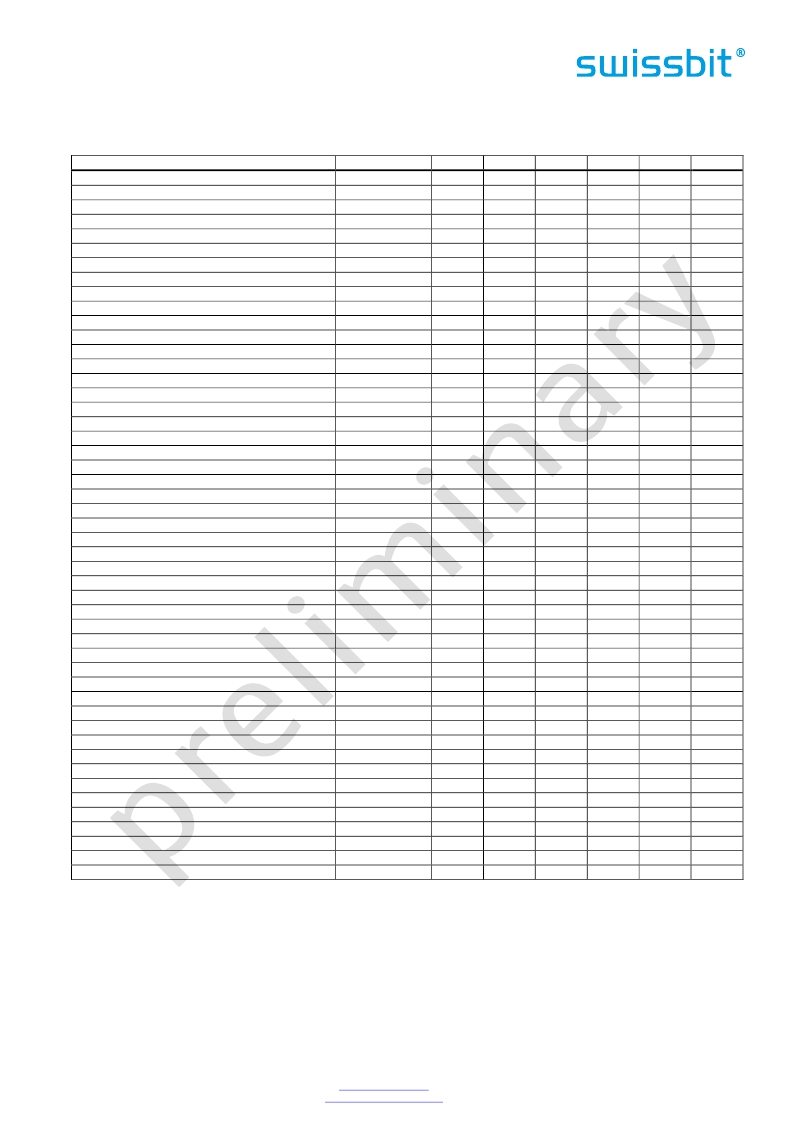
�For� reasons� of� backward� compatibility� some� commands� are� implemented� as� ‘no� operation’� NOP.�
�Table� 13� summarizes� the� Drive� command� set� with� the� paragraphs� that� follow� describing� the� individual�
�commands� and� the� task� file� for� each.�
�Table� 13:� ATA� Command� Set� (1)�
�Command�
�Code�
�FR(1)�
�SC(2)�
�SN(3)�
�CY(5:4)�
�DH(6)�
�LBA(5:3)�
�Check� Power� Mode�
�E5h� or� 98h�
�D�
�Data� Set� Management�
�Execute� Drive� Diagnostic�
�Flush� cache�
�Flush� cache� Ext�
�06h�
�90h�
�E7h�
�EAh�
�YY�
�D�
�D�
�D�
�D�
�YY�
�Format� track�
�50h�
�Y�
�Y�
�Y�
�Y�
�Identify� Drive�
�ECh�
�D�
�Idle�
�Idle� Immediate�
�Media� Lock�
�Media� Unlock�
�NOP�
�Read� Buffer�
�E3h� or� 97h�
�E1h� or� 95h�
�DEh�
�DFh�
�00h�
�E4h�
�Y�
�D�
�D�
�D�
�D�
�D�
�D�
�Read� DMA�
�Read� DMA� Ext�
�C8�
�25h�
�Y�
�YY�
�Y�
�Y�
�Y�
�D�
�Y�
�YY�
�Read� FPDMA� Queued�
�Read� Multiple�
�60h�
�C4h�
�Y�
�Y�
�Y�
�Y�
�Y�
�Y�
�Y�
�D�
�Y�
�Y�
�Y�
�Read� Multiple� Ext�
�Read� native� max� address�
�Read� native� max� address� Ext�
�29h�
�F8h�
�27h�
�YY�
�D�
�D�
�D�
�YY�
�Read� Sector(s)�
�Read� Sector(s)� Ext� 2)�
�Read� Verify� Sector(s)�
�Read� Verify� Sector(s)� Ext�
�20h�
�24h�
�40h� or� 41h�
�42h�
�Y�
�YY�
�Y�
�YY�
�Y�
�YY�
�Y�
�YY�
�Y�
�YY�
�Y�
�YY�
�Y�
�D�
�Y�
�D�
�Y�
�YY�
�Y�
�YY�
�Recalibrate�
�Security� Disable� Password�
�Security� Erase� Prepare�
�Security� Erase� Unit�
�Security� Freeze� Lock�
�Security� Set� Password�
�Security� Unlock�
�1Xh�
�F6h�
�F3h�
�F4h�
�F5h�
�F1h�
�F2h�
�D�
�D�
�D�
�D�
�D�
�D�
�D�
�Seek�
�Set� Features�
�7Xh�
�EFh�
�Y�
�Y�
�Y�
�Y�
�D�
�Y�
�Set� max� address�
�Set� max� address� Ext�
�F9h�
�37h�
�Y�
�YY�
�Y�
�YY�
�Y�
�YY�
�Y�
�D�
�Y�
�YY�
�Set� Multiple� Mode�
�Set� Sleep� Mode�
�C6h�
�E6h� or� 99h�
�Y�
�D�
�D�
�S.M.A.R.T.�
�B0h�
�Y�
�Y�
�Y�
�D�
�Stand� By�
�Stand� By� Immediate�
�Write� Buffer�
�E2h� or� 96h�
�E0h� or� 94h�
�E8h�
�D�
�D�
�D�
�Write� DMA�
�Write� DMA� Ext�
�Write� FPDMA� Queued�
�Write� Multiple�
�Write� Multiple� Ext�
�Write� Sector(s)�
�Write� Sector(s)� Ext�
�Write� Verify�
�CAh� or� CBh�
�35h�
�61h�
�C5h�
�39h�
�30h�
�34h�
�3Ch�
�Y�
�YY�
�Y�
�Y�
�YY�
�Y�
�YY�
�Y�
�Y�
�YY�
�Y�
�Y�
�YY�
�Y�
�YY�
�Y�
�Y�
�YY�
�Y�
�Y�
�YY�
�Y�
�YY�
�Y�
�Y�
�D�
�D�
�Y�
�D�
�Y�
�D�
�Y�
�Y�
�YY�
�Y�
�Y�
�YY�
�Y�
�YY�
�Y�
�1.�
�2.�
�FR� =� Features� Register� (1),� SC� =� Sector� Count� Register� (2),� SN� =� Sector� Number� Register� (3),� CY� =� Cylinder�
�Registers� (5:4),�
�DH� =� Drive/Head� Register� (6),� LBA� =� Logical� Block� Address� Mode� Supported� (see� command� descriptions� for�
�use),�
�Y� –� The� register� contains� a� valid� parameter� for� this� command.� For� the� Drive/Head� Register� Y� means� both� the�
�Drive� and� head� parameters� are� used.�
�YY� –� registers� must� be� written� twice� for� 48bit� LBA� commands�
�D� –� only� the� Drive� parameter� is� valid� and� not� the� head� parameter� C� –� the� register� contains� command�
�specific� data� (see� command� descriptors� for� use).�
�To� read� out� the� higher� and� lower� byte� of� the� 16bit� registers� bit7� of� the� Device� Control� Register� (write� to�
�Alternate� status� register)� must� be� set� to� 1� or� 0,� respectively.�
�Swissbit� AG�
�Industriestrasse� 4�
�Swissbit� reserves� the� right� to� change� products� or� specifications� without� notice.�
�Revision:� 0.92�
�CH-9552� Bronschhofen�
�Switzerland�
���F-240_data_sheet_CA-HxBV_Rev092.doc�
�Page� 15� of� 56�
�发布紧急采购,3分钟左右您将得到回复。
相关PDF资料
SFCF2048H1BO2TO-I-M0-523-SMA
FLASH SLC UDMA/MDMA/PIO 2G
SFCF4096H4BK2SA-I-QT-553-SMA
FLASH SLC UDMA/MDMA/PIO 4G
SFCF64GBH2BU4TO-I-NU-517-STD
FLASH SLC UDMA/MDMA/PIO 64GB
SFN08B4702CBQLF7
RES ARRAY 47K OHM 7 RES 8-DFN
SFP1050-12BG
FRONT END AC/DC 1050W 12V
SFP450-12BG
PWR SUP 450W 12V 36.6A W/STANDBY
SFSD1024N1BN1TO-I-DF-151-STD
FLASH MICRO SD CARD IND S-200 1G
SFSD2048L1BN2TO-I-DF-151-STD
FLASH SECURE DGTL CARD SD 2G
相关代理商/技术参数
SFCA8192H1BR4TO-C-DT-236-STD
制造商:SWISSBIT NA INC 功能描述:FLASH
SFCA8192H1BR4TO-I-DT-226-STD
功能描述:FLASH CFAST CARD UDMA F-100 8GB RoHS:是 类别:存储卡,模块 >> 存储器,PC 卡 系列:F-100 标准包装:30 系列:- 存储容量:8GB 存储器类型:存储卡 - Extreme III SD?
SFCA8192H1BR4TO-I-DT-236-STD
功能描述:FLASH CFAST UDMA/MDMA/PIO 8GB RoHS:是 类别:存储卡,模块 >> 存储器,PC 卡 系列:F-100 标准包装:30 系列:- 存储容量:8GB 存储器类型:存储卡 - Extreme III SD?
SFCA8192H2BV4TO-C-DT-216-STD
制造商:SWISSBIT NA INC 功能描述:FLASH
SFCA8192H2BV4TO-C-DT-226-STD
制造商:SWISSBIT 功能描述:CFAST F-240 DENSITY COMMERCIAL - Trays
SFCA8192H2BV4TO-I-DT-216-STD
功能描述:FLASH CFAST UDMA/MDMA/PIO 8GB RoHS:是 类别:存储卡,模块 >> 存储器,PC 卡 系列:F-240 标准包装:30 系列:- 存储容量:8GB 存储器类型:存储卡 - Extreme III SD?
SFCA8192H2BV4TO-I-DT-226-STD
制造商:SWISSBIT 功能描述:CFAST F-240 DENSITY INDUSTRIAL - Trays
SFCC-4-01
功能描述:CABLE CLAMP SPLIT FLAT #4 SCREW RoHS:是 类别:线缆,导线 - 管理 >> 线夹和夹具 系列:- 标准包装:100 系列:TC 类型:C-夹 开口尺寸:0.79" L x 0.54" W x 0.67" H(20.1mm x 13.7mm x 17.0mm) 安装类型:钉子 材质:聚丙烯 颜色:黑